
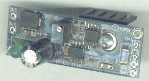
(DCPCB) Spec Page
General:
- This small driver board will drive
many laser diodes currently on the market as well as higher
voltage diodes.
- Available in 1.5 A output (DCPCB)
or 150 mA output (DCPCB-2 on other
spec page)
- 10 Turn Potentiometer for precision adjustment of current.
- Test Points for monitoring of actual Optput Current.
- Can be utilized to drive other loads including TE Coolers, Resistive heaters, etc.
- TO- 220 type output device with Heat Sink.
- ~ 2" X 3/4 " with mounting hols.
- MADE IN USA
DATA SHEET:
DCPCB , 1.5 Amp Driver 
Files in .pdf
You must utilize Adobe® Reader® or other
software
to view the data sheet.
To download a FREE copy of Adobe®
Reader®, click
logo below:
![]()
Adobe®, and Adobe® Reader® are
registered
trademarks of Adobe Systems Incorporated. All rights reserved.
BUY DCPCB NOW
with Paypal LINK BELOW:
Add
multiple lenses
and/ or other items to cart.
No added ship fees for 10 or less items !
Add
this
item to your
cart, buy multiple items, and return to shopping- all choices available.
This page last modified 1 September, 2011